 |
|
CDCLVD2102RGTT
There is sufficient supply and we are currently supplying... |
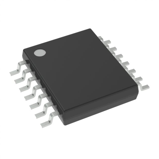
| The CDCLVD2102 clock buffer distributes two clock inputs (IN0, IN1) to a total of 4 pairs of differential LVDS clock outputs (OUT0, OUT3). Each buffer block consists of one input and 2 LVDS outputs. The inputs can either be LVDS, LVPECL, or LVCMOS.
T... |
|
| Chip Information |
|
|
| Model |
|
CDCLVD2102RGTT |
| Brand |
|
TI |
| PDF |
|
Viewing PDF files |
| Inventory quantity |
|
19761 |
| Characteristic |
|
|
| Minqty |
|
VQFN (RGT) | 16 |
| Packaging |
|
250 | SMALL T&R |
| Temperature |
|
-40 to 85 |
| Describe |
|
| |
| The CDCLVD2102 clock buffer distributes two clock inputs (IN0, IN1) to a total of 4 pairs of differential LVDS clock outputs (OUT0, OUT3). Each buffer block consists of one input and 2 LVDS outputs. The inputs can either be LVDS, LVPECL, or LVCMOS.
The CDCLVD2102 is specifically designed for driving 50- transmission lines. If driving the inputs in single ended mode, the appropriate bias voltage (VAC_REF) should be applied to the unused negative input pin.
Using the control pin (EN), ou |
| |
|
| Previous article |
 |
| TLC555CD |
| Texas Instruments |
| TLC555 是一款采用 TI LinCMOS... |
|
|
| Next article |
|
| CDCE62005RGZR |
| Texas Instruments |
| The CDCE62005 is a high performance... |
|
|
|